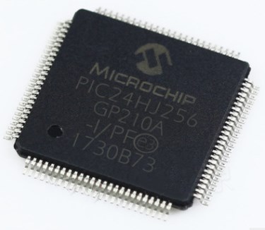
Crack MCU / Read mcu code for PIC24HJ256GP/Extract IC program
The PIC24HJ256GP device family includes devices with different pin counts (64 and 100 pins), different program memory sizes (64 Kbytes, 128 Kbytes and 256 Kbytes) and different RAM sizes (8 Kbytes and 16 Kbytes).
This makes these families suitable for a wide variety of high-performance digital signal control applications. The devices are pin compatible with the dsPIC33F family of devices, and also share a very high degree of compatibility with the dsPIC30F family devices. This allows easy migration between device families as may be necessitated by the specific functionality, computational resource and system cost requirements of the application.
The PIC24HJ256GP device family employs a powerful 16-bit architecture, ideal for applications that rely on high-speed, repetitive computations, as well as control.
Crack MCU / Read mcu code for PIC24HJ256GP/Extract IC program pleast contact unlockmcu@gmail.com
The 17 x 17 multiplier, hardware support for division operations, multi-bit data shifter, a large array of 16-bit working registers and a wide variety of data addressing modes, together provide the PIC24HJ256GP Central Processing Unit (CPU) with extensive mathematical processing capability. Flexible and deterministic interrupt handling, coupled with a powerful array of peripherals, renders the PIC24HJ256GP devices suitable for control applications. Further, Direct Memory Access (DMA) enables overhead-free transfer of data between several peripherals and a dedicated DMA RAM. Reliable, field programmable Flash program memory ensures scalability of applications that use PIC24HJ256GP devices.
Key Features
Modified Harvard architecture
C compiler optimized instruction set
16-bit wide data path
24-bit wide instructions
Linear program memory addressing up to 4M instruction words
Linear data memory addressing up to 64 Kbytes
71 base instructions: mostly 1 word/1 cycle
Sixteen 16-bit General Purpose Registers
Flexible and powerful Indirect Addressing modes
Software stack
16 x 16 multiply operations
32/16 and 16/16 divide operations
Up to ±16-bit data shifts
8-channel hardware DMA
2 Kbytes dual ported DMA buffer area (DMA RAM) to store data transferred via DMA:
Allows data transfer between RAM and a peripheral while CPU is executing code (no cycle stealing)
Most peripherals support DMA
Up to 40 MIPS operation (at 3.0-3.6V):
Industrial temperature range (-40°C to +85°C)
Low-power, high-speed Flash technology
Fully static design
3.3V (±10%) operating voltage
Industrial temperature
Low-power consumption